
Video unavailable
This video can't be played right now.
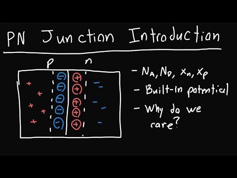
PN Junction Introduction
If you've felt like the content here has been helpful, please consider donating to UCI with a mention of this channel: https://give.uci.edu/ In this video I introduce the P/N junction: the most fundamental device on which all of modern electronics is built. I explain what happens when you put together a piece of N and P-type material, and why the resultant depletion region is formed. This is part of my series on semiconductor physics (often called Electronics 1 at university). This is based on the book Semiconductor Physics and Devices by Donald Neamen, as well as the EECS 170A/174 courses taught at UC Irvine. Hope you found this video helpful, please post in the comments below anything I can do to improve future videos, or suggestions you have for future videos.
Suggested videos
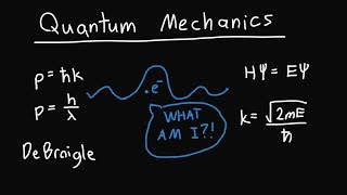
Quantum Mechanics Basics
Jordan Edmunds Chetty · 10:09

PN junction Diode Explained | Forward Bias and Reverse Bias
ALL ABOUT ELECTRONICS · 14:50
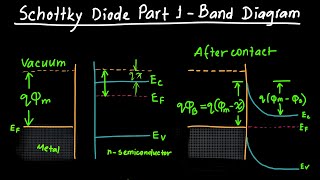
Schottky Diode Part 1 - Band Diagram
Jordan Edmunds Chetty · 11:32

The PN junction | Semiconductors | Class 12 | Physics | Khan Academy
Khan Academy India - English · 10:06

How does a diode work - the PN Junction (with animation) | Intermediate Electronics
CircuitBread · 5:03
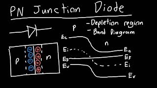
PN Junction Diode Introduction
Jordan Edmunds Chetty · 13:07
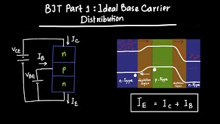
BJT Explained Part 1 - Ideal Base Carrier Distribution
Jordan Edmunds Chetty · 11:53

PN Junction Diode (No Applied Bias)
Neso Academy · 18:31
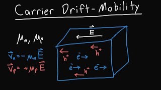
Carrier Drift Current: Mobility
Jordan Edmunds Chetty · 11:23

Topic 1: Introduction to PN Junction Diodes
Electronics for Guitarists · 24:05

Solar Cell Circuit Model Explained
Jordan Edmunds Chetty · 9:05

Diodes Explained - The basics how diodes work working principle pn junction
The Engineering Mindset · 11:32